

Samsung to use TSMC tech for Nvidia’s next-generation memory chips, says Seoul newspaper
The move marks the first time the two companies have worked together at the manufacturing stage
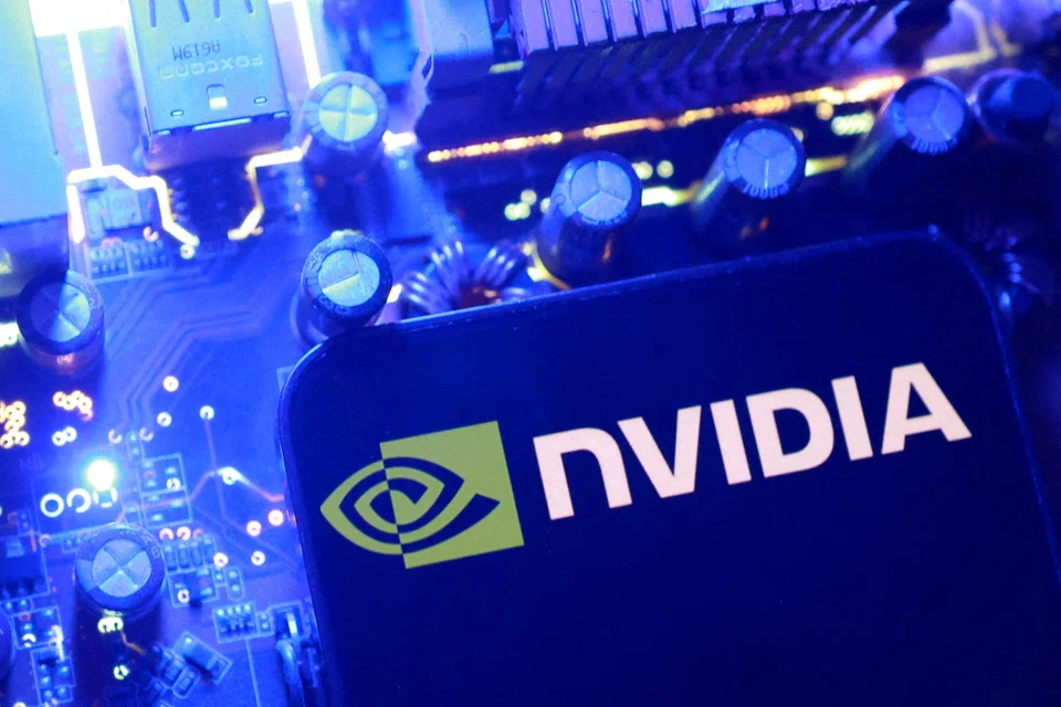
[SEOUL] Samsung Electronics will use TSMC’s 3-nanometre process to produce base dies for Nvidia’s next-generation custom high-bandwidth memory (HBM) chips, the Seoul Economic Daily reported on Sunday (Oct 18).
The move would mark the first time Samsung has worked with the Taiwanese contract chipmaker at the HBM manufacturing stage, according to the report.
Nvidia has asked Samsung, SK Hynix and Micron Technology to use TSMC’s process for Nvidia HBM (NVHBM) base dies, and sixth-generation Dram technology for its core dies, the newspaper said, citing industry sources.
NVHBM, unveiled in August, integrates Nvidia’s custom memory controller into the base die and is aimed at standardising implementation across multiple memory suppliers, said the company.
Samsung accepted Nvidia’s requirements after an internal review, but plans to retain its in-house production model for standard HBM and custom products for other customers, Seoul Economic Daily said.
It is also assessing whether its foundry could produce NVHBM base dies if demand exceeds TSMC’s capacity, the newspaper quoted an unnamed source as saying. REUTERS
Decoding Asia newsletter: your guide to navigating Asia in a new global order. Sign up here to get Decoding Asia newsletter. Delivered to your inbox. Free.
Share with us your feedback on BT's products and services
TRENDING NOW

Cracks emerge in AI borrowing boom as CoreWeave, Oracle and SoftBank debt worries grow

Could stablecoins be the future of money?

‘How many will survive?’: Bubble fears arise as China’s humanoid robotics face reality check

Philippine power giant First Gen rebuffs foreign offers, plans up to US$2.6 billion in expansion

