Samsung Electronics breaks ground on new chip R&D centre, plans 20t won investment by 2028
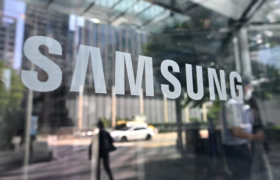
SAMSUNG Electronics said on Friday it broke ground at a new semiconductor research and development (R&D) complex in South Korea, where it plans to invest about 20 trillion won (S$20.8 billion) by 2028 to drive leadership in chip technology.
The world’s largest memory chip maker and second-largest chip contract manufacturer said the new facility at Giheung, south of Seoul, will lead advanced research on next-generation devices and processes for memory and system chips, as well as development of new tech based on a long-term roadmap.
“Samsung Electronics is seeking to overcome the limits of semiconductor scaling,” it said in a statement.
The groundbreaking ceremony was attended by newly-pardoned Samsung Electronics vice-chairman Jay Y. Lee and top executives.
“We need to continue our tradition of investing pre-emptively and emphasizing technology,” Lee said during the ceremony.
Lee later met chip business employees and separately met with executives to discuss ways to secure technology to expand semiconductor leadership, Samsung said. REUTERS
Decoding Asia newsletter: your guide to navigating Asia in a new global order. Sign up here to get Decoding Asia newsletter. Delivered to your inbox. Free.
Share with us your feedback on BT's products and services