

Why Huawei’s new chipmaking plan has investors buzzing
The company’s vision for improving semiconductor efficiency has sparked a rally across the sector in China
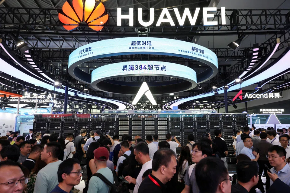
[SHENZHEN] The artificial intelligence boom has triggered an insatiable demand for computing power, with companies such as Amazon, Meta Platforms and Microsoft pouring hundreds of billions of dollars into data centres and advanced chips developed by US semiconductor giant Nvidia.
China, meanwhile, is at risk of falling behind in the AI race as US trade restrictions limit its access to critical chipmaking technology.
Against that backdrop, Chinese tech giant Huawei Technologies captivated industry watchers and investors on Monday (May 25) when its semiconductor chief He Tingbo outlined a new approach to chip design – a departure from the decades-long industry focus on shrinking transistors to improve performance.
The company’s vision for improving semiconductor efficiency, which it calls Tau Scaling Law, sparked a rally across China’s chipmaking sector the following day.
Investors bet on Huawei’s ability to innovate within the constraints imposed by US trade curbs, pushing shares of its chipmaking partner Semiconductor Manufacturing International Corporation (SMIC) up nearly 6 per cent.
What do we know about Huawei’s plan?
Decades ago, Intel co-founder Gordon Moore predicted that advancements in semiconductor manufacturing would allow the number of transistors in an integrated circuit to roughly double every couple of years.
This observation, which became known as Moore’s Law, held true for decades as smaller transistors on more densely packed circuits boosted performance while consuming less power.
Huawei’s proposed Tau Scaling Law seeks to move away from that model by improving performance not through ever-shrinking transistors, but by shortening the distance that data must travel inside a processor.
The company has called this technology LogicFolding: dividing what would typically be a flat chip layout into slices of computing blocks and stacking them atop each other so information can move more quickly.
SEE ALSO





The concept isn’t new; chip designers including industry leader Taiwan Semiconductor Manufacturing Co (TSMC) already use advanced stacking technologies. But Huawei is proposing a more aggressive redesign of chip architecture itself.
Such an approach could face significant engineering challenges, including manufacturing complexity, heat dissipation and power delivery. It also remains to be seen whether the technology can be deployed economically and at scale.
Nevertheless, Huawei has outlined an ambitious road map for LogicFolding and said that it plans to introduce the first such chips in smartphones later this year.
He Hui, a Shanghai-based analyst at global technology research and advisory firm Omdia, noted that Huawei has little to lose by pursuing this new approach, given that the company is already at the physical limits of what its available technology can do.
What would make such a breakthrough so significant?
Huawei is currently operating near the physical limits of the manufacturing technology available to it.
The company is effectively constrained to producing chips at a geometry of 7 nanometres (nm) because US-led export restrictions have cut off its access to the extreme ultraviolet lithography systems needed to pattern ever-smaller transistors efficiently and at scale.
If successful, such a breakthrough could allow Huawei to work around these trade restrictions by improving chip performance through design and packaging innovation, rather than through technology that it doesn’t have access to.
This could help narrow the technological gap with rivals such as TSMC. With LogicFolding, Huawei said it aims to produce semiconductors with performance comparable to 1.4 nm chips by 2031.
That would still leave Huawei years behind TSMC, which is targeting similar advances by 2028, but it would represent a substantially narrower gap than what exists today. Huawei and its manufacturing partner SMIC are currently several generations behind the Taiwanese chipmaker.
What are the possible challenges with LogicFolding?
Adding more layers to a chip stack significantly increases manufacturing complexity and raises the likelihood of defects, potentially reducing the yield of commercially viable chips.
The stacking approach could also create major thermal challenges, as densely layered chips tend to trap more heat and may require more advanced cooling systems. One major advantage of flat chips is the maximal surface area for heat dissipation.
Why has the US restricted China’s access to its chipmaking technology?
Both the United States and China view advances in AI as strategically important not only economically but also militarily, and Washington is intent on preserving its lead over Beijing in this field.
Successive US administrations from both political parties have steadily expanded export restrictions on China, targeting not just advanced AI chips but also the tools and machines needed to make them.
US officials argue that limiting China’s access to cutting-edge semiconductors could slow its development of advanced military, surveillance and defence capabilities.
At the same time, some US policymakers and industry executives – including Nvidia CEO Jensen Huang – have argued that restricting access could ultimately backfire by spurring Chinese rivals to accelerate their own technological development. BLOOMBERG
Decoding Asia newsletter: your guide to navigating Asia in a new global order. Sign up here to get Decoding Asia newsletter. Delivered to your inbox. Free.
Share with us your feedback on BT's products and services
TRENDING NOW

DBS, OCBC, UOB rout lops billions off STI as inflation, rate concerns spook investors

Grab CEO’s wife Chloe Tong on life with Anthony Tan and finding her purpose

OCBC sheds S$8 billion in value as shares close nearly 6% down; analysts cautious on banks

Deal between tycoon friends sparks scrutiny of Philippine power sector

